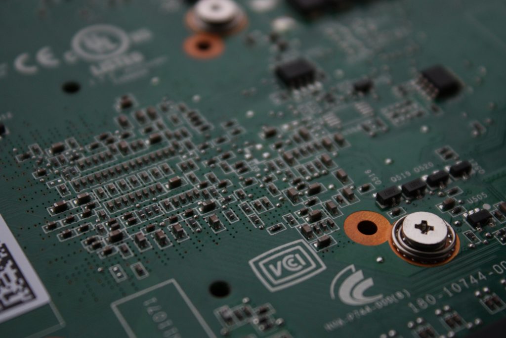
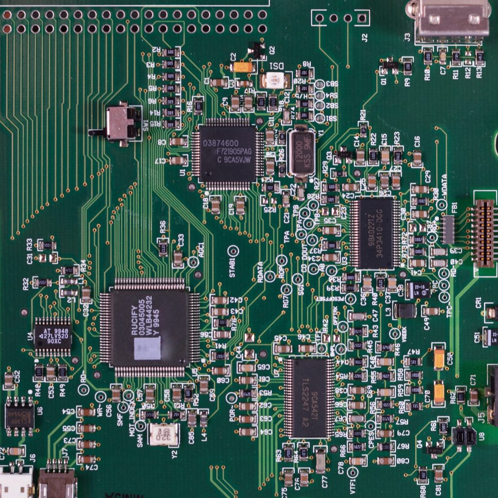
In the ever-evolving landscape of modern technology, semiconductors play a pivotal role as the building blocks of electronic devices. As these devices become increasingly intricate and advanced, the need for rigorous testing and quality control has never been greater.
Among the array of testing techniques available, light analysis is a powerful tool for ensuring the performance, reliability, and consistency of semiconductor components. In this blog post, we’ll explore the significance of light analysis in semiconductor testing, its underlying principles, and its applications in ensuring the integrity of these crucial components.
Understanding Light Analysis in Semiconductor Testing
Light analysis, also known as optical metrology, involves the use of light to characterize and measure various properties of materials, surfaces, and structures. In the context of semiconductor testing, light analysis techniques provide valuable insights into parameters such as thickness, composition, stress, and defects. By leveraging the interaction between light and semiconductor materials, engineers can extract precise information that aids in manufacturing optimization and quality assurance.
Principles of Light Analysis in Semiconductors
Reflectance and Transmittance Spectroscopy: Reflectance and transmittance spectroscopy are commonly used techniques in semiconductor testing. By measuring the amount of light reflected or transmitted through a semiconductor sample, engineers can determine properties such as layer thickness, refractive index, and absorption characteristics.
Ellipsometry: Ellipsometry measures changes in the polarization state of light reflected from a sample. It provides information about film thickness, optical constants, and even the electrical properties of semiconductor layers.
Photoluminescence Spectroscopy: This technique involves exciting a semiconductor sample with light and then measuring the emitted light (photoluminescence) that is produced. It’s particularly useful for analyzing the quality of semiconductor materials, detecting defects, and understanding carrier recombination processes.
Applications of Light Analysis in Semiconductor Testing
Thin Film Characterization: Light analysis techniques are crucial for characterizing thin films used in semiconductor fabrication. They enable engineers to measure layer thickness, uniformity, and composition, which are essential for ensuring the performance of transistors, capacitors, and other semiconductor components.
Defect Detection: Light analysis can detect defects and irregularities in semiconductor materials and structures. Photoluminescence spectroscopy, for example, can identify defects and impurities that affect the semiconductor’s electronic properties.
Stress and Strain Analysis: By measuring changes in the way light interacts with a semiconductor under stress, engineers can assess mechanical stress and strain in the material. This is crucial for ensuring the structural integrity of semiconductor devices.
Wafer Inspection: Light analysis techniques are used for wafer inspection at various stages of the manufacturing process. They help identify surface defects, contamination, and inconsistencies that could affect device performance.
Benefits of Light Analysis
Non-Destructive: Light analysis techniques are non-destructive, meaning they can provide detailed insights into semiconductor properties without altering or damaging the sample.
High Precision: Light analysis offers high precision and accuracy, enabling engineers to make informed decisions about manufacturing processes and quality control.
Speed and Efficiency: Light analysis techniques are relatively fast, allowing for high-throughput testing in semiconductor production facilities.
Light analysis has revolutionized semiconductor testing by providing a non-invasive, accurate, and efficient way to assess the properties and quality of semiconductor materials and components. From thin film characterization to defect detection, the insights gained through light analysis techniques are indispensable in maintaining the high standards required in today’s semiconductor industry. As technology continues to advance, so does the role of light analysis in shaping the future of electronic devices.